Isolation milling can be used for producing prototypes and small PCB productions.
The advantage of isolation milling above the conventional way of using chemicals is obvious.
Less chemicals = less pollution. It also prevents chemical hazards . This is especially true
for students who are in majority not to concerned in handling chemicals the proper way.
Another big advantage is the speed in which you can make a prototype, you do not have
to wait for some PCB manufacturer to get your prototypes ready and then find out there are
still design errors.
Isolation milling is making grooves around traces to isolate them.
After all copper is removed around the different nets (connected copper objects),
the electrical connectivity will be the same as when the PCB was etched.
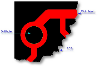
The majority of the copper remains on the board which in some case can be used as a ground plane. Because PCB design software produce Gerber or HPGL data we need to calculate the isolation patterns. This is were Engraver © comes in. As you will become familiar with the program you'll discover many handy features you may use for your projects. Before you start milling your design looks like this: (please note that different layers use different colors) |
|
|
|
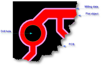
After milling your board might look like this:
The black and red area's represents the copper that is left. The pink lines separate the red and black area's, representing the isolation.
|
|